


 English (pdf)
 Article in xml format
 Article references
 Send this article by e-mail
 Cited by SciELO
  Similars in
SciELO
Similars in
SciELO 
 Permalink
Introduction
Fifteen years ago, O’Regan and Grätzel (1991) introduced a new photoelectrochemical, practical, low cost device, which he named dye-sensitized solar cell (DSSC). In such DSSC, a nanocrystalline semiconductor layer sensitized with dyes on conductive glass composes the photoanode; which is permeated by an electrolytic solution containing the redox couple I3 - / I-, and the thin solar cell is completed by a second layer of glass deposited platinum acts as counter electrode (see Figure 1 for a scheme of the process). (Peter, 2007)
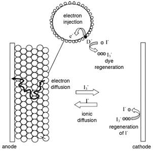
Figure 1 Key processes involved in the regenerative cycle happening in the dye-sensitized solar cell under illumination. Taken from Peter, 2007.
It is of great interest to find substitutes for the commonly transparent conductive materials, fluorine and indium tin oxides (FTO and ITO) in the electrodes of DSSC, since it accounts for about 80% of the cost of the cells (Ito & Takahashi, 2012) and is very brittle, remaining the main limitation for fabricating flexible devices (Dong et al., 2014).
Graphene, a monolayer of sp2-bonded carbon atoms, is a quasi-two-dimensional (2D) material that possesses great electrical and optical properties (Li et al, 2009), making it very attractive for this purpose. It has shown an outstanding thermal conductivity, remarkable mobility of charge, excellent mechanical strength, high transparency, high specific surface area and adjustable structures. (Ibadurrohman and Hellgardt, 2014) From the many methods for obtaining graphene, the technique for growing it by CVD on copper foils results of major importance, since it can be applied to large-scale production. The films grow directly on the surface by the catalytic activity of the Cu and the obtained film is graphene with one, two or few-layer thickness. The annealing of Cu previous to the growing step, leads to very large domains of the graphene, which is a limiting factor in other metals like Ni. (Li et al, 2009)
Raman shift spectroscopy fingerprints for single, double layers and some layers allow nondestructive identification of graphene layers unequivocally and reflect changes in the electron band (Ferrari et al, 2006). As shown in Figure 2C, graphene material has two main peaks, G (1600cm-1) and 2D (2600cm-1), which could derive in three cases a) if the G peak is less than the 2D intensity, the graphene is one layer thick, b) if the two peaks have the same intensity, the material obtained is bilayer graphene, and c) if the G is greater than the 2D, it corresponds to few layer graphene. (Li et al, 2009)
Zinc oxide (ZnO) is an n-type semiconductor material with a wide functional single bandgap (3.37 eV) at room temperature (Nouneh et al, 2015), and an effective ultraviolet luminescence (Özgür et al., 2005). Quasi-one-dimensional structures (1D) as nanowires and nanorods, zinc oxide are promising materials for nanoelectronics (Park et al., 2005), and have great potential for applications in sensors and photovoltaic devices (Nouneh et al, 2015). The synthesis of graphene-ZnO hybrids and their applications in DSSC have been reviewed in our group previously (Badhulika et al. 2015).
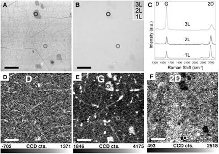
Figure 2 A.SEM images, B. Optical image, C. Raman spectroscopy and D. Raman maping of graphene layer. Taken from Li et al, 2009.
When characterizing the performance of DSSC, the standard procedure is to measure the current density vs. voltage curve, also known as J-V curve. In this method, the anode and cathode of the cell are connected to a power source, the cell is illuminated, and a voltage sweep is applied while the current is measured. This method provides limited information of the intricate processes that are taking place in the cell. Electrochemical impedance spectroscopy (EIS) is a complementary technique that allows getting insight into the charge transport, transfer and accumulation mechanisms taking place in the cell (Sarker 2014). The Nyquist plots obtained with EIS of the imaginary impedance versus the real impedance of the cell have been well understood to interpret the internal impedance elements of the cell. Nyquist plots usually exhibits three semicircles, which are attributed a) to the redox reaction at the counter electrode in the high frequency region, b) to the electron transfer interface in the semiconductor / dye / electrolyte in the middle region and c) to the carrier transport frequency by ions into the electrolyte in the low frequency region.
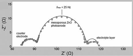
Figure 3 Nyquist plot of a DSSC obtained by electrochemical impedance spectroscopy (Abdullah et al, 2015)
The model diagram of the equivalent circuit for a DSSC shown in Figure 4 consists of the following elements (Manoharan and Venkatachalam, 2014):
The series resistance (Rs) starting point of the first semicircle in the Nyquist diagram.
The electron transport resistance in the counter electrode / electrolyte (Rct) first semicircle first Nyquist plot presented in the high frequency region.
The resistance to charge transfer at the photoanode / dye / electrolyte interface (Rrec) second semicircle Nyquist diagram presented in the middle frequency region.
The constant phase elements of capacitance for each resistor Crec capacitance (Rrec), Cct
(Rct).
Warburg diffusion impedance Zd, presented in the low frequency region.
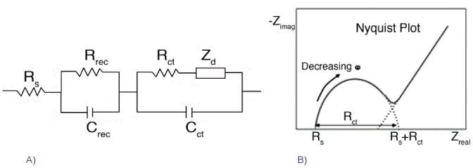
Figure 4 a) Equivalent circuit similar to that DSSC posed configuration. (Taken from Manoharan and Venkatachalam, 2014). b) Scheme of the equivalent circuit components seen in the Nyquist plot.
Other solid state measurements that require the fabrication of simple devices are also helpful in quantifying the electrical transport through the solid materials and interfaces of the cell, for example, field effect transistors.
Experimental details
Graphene synthesis and transfer
A 1 in2 copper foil piece, Alfa Aesar 99.999% 25 μm thick, is cleaned by immersing during 10min sequentially in 40 ml of 5%v/v acetic acid, then in DI water, followed by acetone and finally isopropyl alcohol. The copper foil is carefully dried with N2 without making wrinkles, and then placed on a quartz holder inside a quartz tube in a furnace, model Linberg Blue M from Thermo Scientific 1” diameter. The tube is purged with Ar and H2 for 10 min. Then the tube is heated up to 1030˚C under 8 sccm H2 and 190 sccm Ar at a rate of 30˚ C/min and left at that temperature for 30 min to anneal the foil. After annealing, 10 sccm of CH4 are allowed to flow with the H2 and Ar for 12 min for the graphene to grow on the surface. Once the growth is done, the CH4 and H2 are immediately turned off, as well as the furnace, and the sample is left for cooling down under Ar atmosphere to room temperature.
The copper foil with graphene is spin-coated with a thin film of PMMA 4% during 30s at 3000rpm and baked at 100˚C for 3 min. The copper foil is cut in 1 cm2 pieces and placed on top of a
0.3M FeCl3 solution in a petri dish for 3 hours, until the copper is completely dissolved, and a transparent dark film is visible floating on the surface. The FeCl3 solution is carefully replaced by clean water by repetitive pipetting DI water in and out of the petri dish, until the solution loses its yellowish color. Then HCl is added to make up for a 5%v/v concentration and left for 1 hr to remove FeCl3 traces. The HCl is carefully replaced by the same pipetting method until the pH of the water is neutral.
Cut glass slides are used as substrate for the graphene. The glass substrates are cleaned by washing with soap and cotton swabs, sonicating for 10 min with acetone, and immersing in piranha (3:1 H2SO4:H2O2) for 1 hr, to remove organic residues and make the surface hydrophilic. The graphene pieces are scooped carefully with the glass slide and left to air dry, followed by 1hr drying at 50˚C to remove adsorbed water. The samples are then soaked in acetone overnight to remove the PMMA coating. Finally, the samples are annealed in 20 sccm Ar under vacuum (2 mTorr) at 250˚C for 1hr. For multiple-stacked graphene, a second graphene layer was scooped on top of the first on glass by following the same procedure. For doping, graphene samples are immersed in HNO3 65% during 5 min and then rinsed with water.
ZnO Synthesis
The method developed by our group in (Hernández-Valle & Chaves-Villarreal, 2014) was optimized for the growth of VAZNR on graphene by CVD (see Figure 5). A truncated horizontal glass test tube of 1” length containing 50 mg of Zn powder (Alfa Aesar 99,9 %) was placed inside the same tubular furnace described above, with the closed side facing the gas influx. The graphene/glass substrate was placed immediately next to the open side of the tube. The furnace was purged with Ar for 10min, and then heated up to 570˚C at a rate of 50˚C/min under 190 sccm Ar flux. Once the furnace reached that temperature, 4 sccm of air (20% O2, 80% N2) were added to the gas flux and left for ZnO growth during 15 min. After growth, the furnace was turned off and cooled down to room temperature under the same Ar and air flux. The obtained hybrid material was later annealed at 500˚C for 1hr under Ar atmosphere and 1atm pressure.
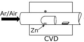
Figure 5 Setup for in situ growth of VAZNR on graphene by CVD (adapted from Hernández-Valle & ChavesVillarreal, 2014)
Materials characterization
Scanning electron microscopy (SEM) of the graphene and of the ZnO/graphene hybrid was performed in a FEI NNS450. Transmission Electron Microscopy (TEM) and Electron Diffraction of the graphene were performed in a FEI CM300. The graphene for TEM was not coated with PMMA, and after Cu etching it was simply scooped with a C-coated Cu grid. Both microscopy characterizations were done in the Central Facility for Advanced Microscopy and Microanalysis of UC Riverside.
To test the electrical conductivity of the graphene, we fabricated two simple devices made up of a 1x1cm2 of graphene transferred on Si/SiO2. The graphene film was protected with thermal release tape [Revalpha, Nitto Denko America Inc.], leaving 2 mm on opposite sides uncovered for overlapping with gold contacts. Gold contacts of 140nm thickness were deposited by e-beam evaporation with a Temescal BJD 1800. The thermal tape was then removed by heating the sample to 110˚C for 5 min. One device was subjected to the ZnO growth by CVD and the other device was subjected to the same conditions of temperature and oxygen concentration but in the absence of Zn powder. The resistance of the devices was measured before and after the two treatments.
DSSC assembly and testing
The fabricated photoanode (VAZNR/graphene) was immersed in an ethanoic solution of 0.3 mM N-3 dye (cis-Bis(isothiocyanato) bis(2,2’-bipyridyl-4,4’-dicarboxylato ruthenium(II)) for 24h. Then it was air dried and assembled in a sandwich-type DSSC (see figure 15 for detail). The counterelectrode was a 5nm Pt film deposited on glass by e-beam evaporation at a rate of 2 Å/s. The electrolyte was composed of 0.1 M LiI and 0.03 M I2 in acetonitrile. 10-20 μl of the electrolyte was placed in between the two electrodes, which were separated by a thermoplastic film (Solaronix, Meltonix 60 μm).
For obtaining the J-V curve and EIS of the cell, a CHI 760C electrochemical workstation was used under 100 mW/cm2 illumination of a Photon Technology International Xe lamp. The photanode is connected as working electrode to the power source, while the Pt glass is connected to the counterelectrode and shunt to the reference. For the J-V curve, a voltage sweep from -1 to 1V was applied. For EIS, the applied bias voltage was set at the open circuit voltage of the DSSC with ac amplitude of 10mV between working electrode and counterelectrode, within a frequency range of 10-2 to 104 Hz.
Results and Discussion
Graphene characterization
The optical micrograph of the graphene on glass is shown in Figure 6a, where it is difficult to distinguish due to the high transparency of the material. Raman spectra taken on randomly selected points (Figure 6b) confirm that the synthesized graphene is continuous and when comparing to figure 2c, we can see it is made of one or two layers of material. By analyzing the ratios of peak 2D (2600 cm-1) to the G peak (1600 cm-1), most sites show similar intensity, which indicates double layer graphene, and some show very high ratios, indicating single layer graphene. Besides, the D peak (1350 cm-1), that relates to defects in the crystal structure, is whether nonexistent or has very small intensity, which demonstrates that the recipe used results in very high quality graphene.
Figure 7a displays the TEM micrograph obtained from a flake of the graphene grown, and just as the optical micrograph, there are no special features to be seen. However, the electron diffraction of the same area (Figure 7b) displays the typical six-fold symmetry expected for graphene and graphite, and the duplicity of the spots indicate a bi-layer graphene, giving more veracity to the identification detailed above.
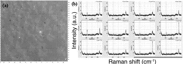
Figure 6 (a) Optical micrograph and (b) its corresponding Raman spectra at different random points of the graphene.

The current vrs voltage curves for a graphene transistor are shown in Figure 8. From the Ids vrs Vds we can extract that the material has an ohmic behavior, due to its semi-metallic nature. The Ids vrs Vg reveal a p-doped material, instead of the expected ambipolar behavior of graphene. However, it is common for CVD-graphene to show such behavior, mainly due to residues left from the transfer with PMMA.
The sheet resistance for graphene depositions is studied after each process steps to determine whether they affect performance. Figure 9 shows similar resistance of about 1200 kΩ for the three different graphene devices having 1, 2 or 3 stacked layers of graphene. After the annealing process, the 1-stacked graphene increases in 600 kΩ its resistance probably due to defects and impurities in the surface. On the other hand, depositions of 2 and 3 layers decreases its sheet resistance due to the annealing, because the imperfections in one layer are counteracted by the next layers, creating a easier pathway for electrons to move. The final step of treatment with nitric acid helps reduce the sheet resistance by incorporating nitrogen atoms in the carbon matrix, which causes an effect of doping in the material. With this form of doping, the electrical conductivity increases
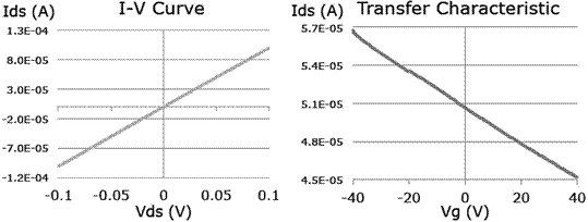
Figure 8 Characteristic electrical curves of drain-source current vrs drain-source voltage and versus gate voltage for a FET transistor. Ids vs. Vds was taken under zero gate voltage. Ids vs. Vg was taken with a Vds 0f 0.1V.
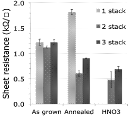
Figure 9 Resistance graphene depositions with 1, 2 or 3 stacked layers and its variation according to the process step.
ZnO-Graphene hybrid
Figure 10 shows top-view and cross-section SEM micrographs of the VAZNR/graphene hybrid. The thickness (t) of the film was about 568±65 nm and the average diameter (d) of the rods was 166±80 nm. The micrograph also displays the vertical alignment obtained by the CVD deposition process described by Hernández-Valle and Chaves-Villarreal.
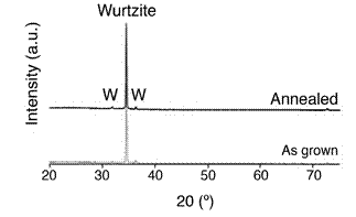
The highly-ordered structure was further confirmed by XRD (fig 11). The pattern can be indexed to the hexagonal wurtzite ZnO structure (JCPDS card no. 36- 1451). A predominant XRD peak is found at 34˚ that corresponds to the (002) planes. This indicates that the VAZNR grow preferentially in the c-direction (along the [0001] direction) perpendicular to the graphene, which makes sense, considering that graphene has a hexagonal structure itself and could promote epitaxial growth of deposited atoms. The peak is very narrow and intense, indicating the high crystallinity of the material. The growth rate along the c-direction increased with temperature more than the growth rate in other directions, reason why long nanorods were obtained.
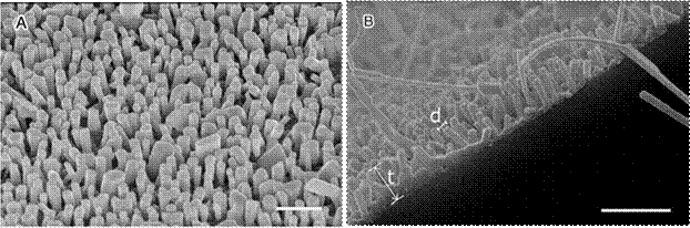
Figure 10 SEM micrograph of (a) top view and (b) cross section of the ZnO nanorods grown on grapheme. Scale bar 1μm.
The highly-ordered structure was further confirmed by XRD (Figure 11). The pattern can be indexed to the hexagonal wurtzite ZnO structure (JCPDS card no. 36- 1451). A predominant XRD peak is found at 34˚ that corresponds to the (002) planes. This indicates that the VAZNR grow preferentially in the c-direction (along the [0001] direction) perpendicular to the graphene, which makes sense, considering that graphene has a hexagonal structure itself and could promote epitaxial growth of deposited atoms. The peak is very narrow and intense, indicating the high crystallinity of the material. The growth rate along the c-direction increased with temperature more than the growth rate in other directions, reason why long nanorods were obtained.
The UV/Vis transmittance spectra was taken for each of the different materials to study their optical properties. Glass has a transmittance of 90-95% and graphene on glass has a transmittance of 70-80%. The peaks of absorbance for the N3 commercial dye in ethanol solution are at 307, 370 and 517 nm. ZnO deposited on graphene/glass shows transmittance of 30-60% and a large absorption around 370m, that corresponds to the energy bandgap of the bulk semiconductor. The ZnO sensitized with N3 dye shows slightly different spectra with slightly larger absorption around 517nm, corresponding to the absorbance of the dye, indicating that the dye is effectively adsorbed on the surface of the semiconductor.
The devices shown in Figure 13 are subjected to two different conditions to determine if the graphene’s electrical conductivity is affected or not by the ZnO deposition. The response before and after is plotted in Figure 14.
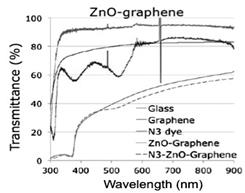
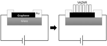
Figure 13 Configuration scheme used for sheet resistance measurements without and with ZnO nanorods on graphene.
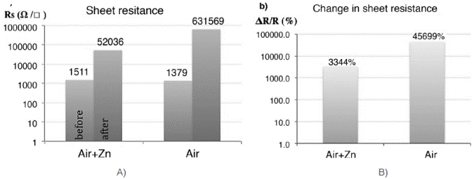
Figure 14 a) Sheet resistance for grapheme before and after exposure to CVD growth conditions and b) change in sheet resistance due to the exposure to CVD growth conditions
Both graphene samples were largely damaged during the CVD reaction. The one exposed to 0.4%v/v air and Zn in the CVD at 570˚C had a 3000% increase of resistance, while for the one that was exposed only to 0.4%v/v air at 570˚C the resistance increased in 46000%. The one that was exposed to ZnO deposition suffered less detriment probably to the protection that the first layers of ZnO provided. Graphene is being oxidized by the small amounts of oxygen that are present in the reaction.
DSSC device
Figure 15 shows a scheme similar to the configuration of the fabricated solar cell. The results of the J-V curve are plotted in Figure 16.
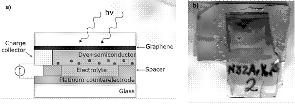
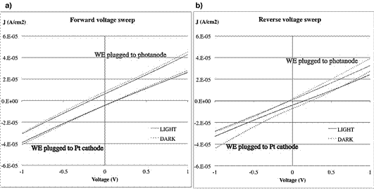
Figure 16 Current density-voltage plots for the solar cells with a) forward voltage sweep and b) reverse voltage sweep.
We observed that for all cases, there is no difference on the current response when the cell is tested in dark or under illumination, neither we see the normal diode curve typical of p-n juntions.
However, there is a linear current response that is shifted from zero at 0V. This can be explained in terms of the polarization of the active layers, were the ions are attracted to the electrodes, and become polarized opposite to the applied field. This creates an internal field. During forward voltage sweep, at -1 the applied field dominates the charge flow, however, as the applied field is reduced, it becomes closer to the internal field, until the current is zero (characteristic crosses at -V, I=0). Then the internal field dominates and the direction of the current is reversed. The current at zero potential occurs due to the induced voltage. In reverse sweep, the same internal field is formed but starting now to be in the opposite direction. The current produced at 0 V is therefore not due to the photocurrent but due to polarization.
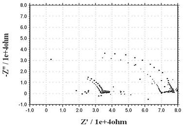
The Rrec, or resistance at the interface graphene/VAZNR/dye, corresponds to the second semicircle in the Nyquist diagram presented in the middle frequency region as seen in Figure 3, and it is of approximately 32 kΩ. This verifies the high resistance that graphene acquire after the process of growing the VAZNR, attaining a resistance in the order of 104 Ω, same order of the resistance measured with the solid state device and shown in Figure 14a. The first semicircle is not visible, due to the very low frequencies at which charge is being transferred in the electrolyte.
Conclusions
The semiconductor material, ZnO, was grown with very high quality on the graphene substrate via CVD method. It grew vertically oriented in the [002] direction with high crystallinity in the wurtzite hexagonal phase. It showed large adsorption of the Ru-based dye. However, the electrical measurements demonstrate that the graphene substrate must have been oxidized during the growth due the exposure to very low amounts of oxygen (0.4%) at high temperatures (570˚C). Therefore, graphene behaves as an excellent sacrificial template for the growth of vertically aligned ZnO nanorods, but it degrades under the growth conditions. The tools of electrical and photoelectrochemical characterization have allowed us to identify the cause of the poor behaviour of the hybrid grown by this method as a photoanode in DSSC

